
Seminar - Semiconductor Field Emission Electron Source
May 24, 11:00, place to be specified
Rupert Schreiner
Ostbayerische Technische Hochschule Regensburg
Semiconductor field emitter arrays are suitable candidates for applications which require a very stable field emission (FE) current and a high emission uniformity over the entire emission area. By using various semiconductor materials, doping profiles, geometries and coatings of the apex it is possible to vary the emission characteristics of these cathodes within a wide range. Each specific application requires its own optimized design for the cathode as
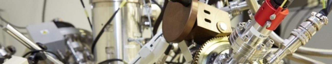
well as for the other parts of the FE electron source. To meet as many of these requirements as possible while using only a limited number of different prefabricated components, we established a modular system concept for our FE electron source. It consists of a semiconductor cathode (with an optional integrated gate electrode) and a grid electrode (metallized silicon nitride membrane). For pre-characterization of the FE electron source, an UHV measurement system is used. An anode is mounted on a movable isolated cantilever and is placed at a defined distance over the extraction grid. Different cathode, gate, grid and anode potentials can be chosen while the corresponding currents are monitored. In addition to the integral FE measurement, the emission characteristics of individual tips out of various cathode materials and using different geometries (e.g. black Si) were investigated by means of FE scanning microscopy. For the actual device application (e.g. vacuum sensor or x-ray source), the electron source can be directly integrated and characterized in the complete system without any further modification.